China’s Quiet Advance in Chipmaking Technology Results in EUV Lithography Machine Breakthrough
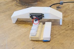
Engineers in a top-secret laboratory in Shenzhen, China, finished building a prototype extreme ultraviolet lithography (EUV) machine this year. We’re hearing from a variety of sources that the item is currently undergoing rigorous testing, which is a huge step forward for domestic chip manufacture. To emphasize the point, the same team has had workers build a similar cutting-edge lithography system from the ground up, demonstrating how large and precise the project truly is.
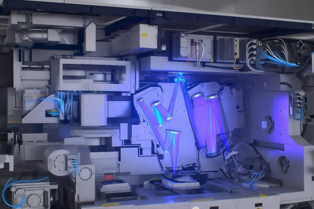
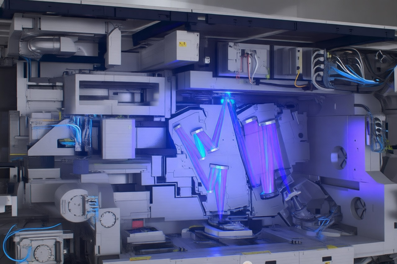
Extreme ultraviolet lithography uses a beam of light with a wavelength of 13.5 nanometers to carve out small patterns on silicon wafers. That is small enough to produce transistors for current processors. Until recently, only one firm, ASML, has been able to commercially build these machines. However, the Chinese researchers adopted a completely different approach when it came to the light source. Scientists from Harbin Institute of Technology created a laser-induced discharge plasma system. They obtain their light by vaporizing a tin target and then blasting it with a high voltage, resulting in a super-hot plasma, which happens to be the exact light they require.
Research centers such as Harbin Institute of Technology are driving the continued development in plasma production and optics. It’s working out well because they’re pursuing a simpler, more energy-efficient path than everyone else. Years of hard work have paid off, with early testing indicating that they have reliable light generation under control.
Huawei is leading the charge in organizing all of this activity, with SMIC and other foundries right in the middle of things. Many former engineers who worked on foreign designs are now providing their knowledge, while domestic institutes do the key optical integration work. The prototype is taking up the entire production floor and producing a variety of test wafers. From here, it’s all about fine-tuning the resolution, ensuring stability, and then putting it all together. They still have some work to do before meeting their government-imposed goal of 2028 to begin producing chips utilizing the method. We might see it go into full commercial operation by 2030, giving them some breathing room to work out the throughput.
All of the constraints on importing foreign equipment have resulted in billions of dollars being poured into research, allowing for advances in light sources and supporting components that were sorely required. They are also reducing the use of earlier multi-patterning systems, which are extremely expensive and inefficient. World leaders are pushing for higher-NA lithography systems, while China is pursuing more cost-effective and reliable alternatives to meet national needs.
[Source]
China’s Quiet Advance in Chipmaking Technology Results in EUV Lithography Machine Breakthrough
#Chinas #Quiet #Advance #Chipmaking #Technology #Results #EUV #Lithography #Machine #Breakthrough